Jump to:
In case you missed it: FinFET Layout Part 1
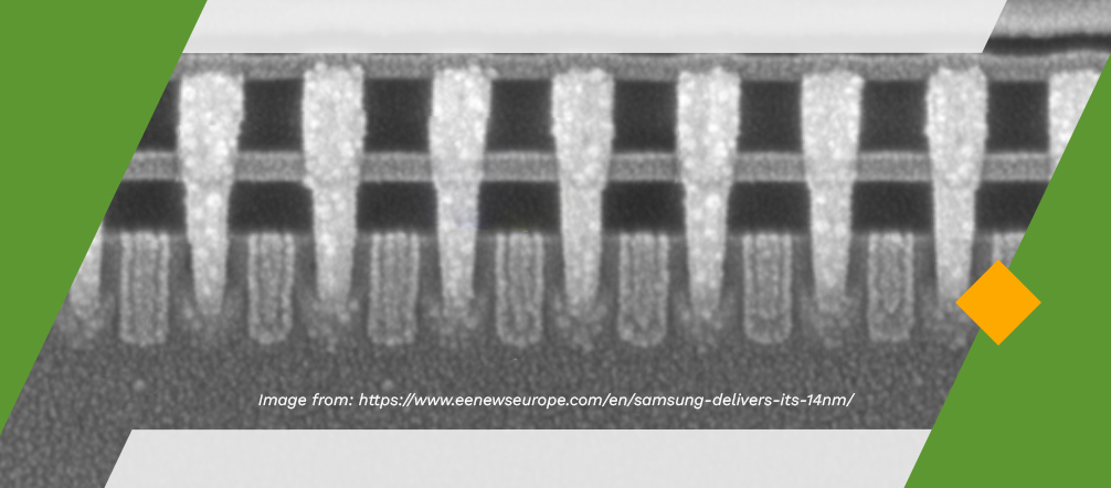
In our last post, we looked at the basics of finFET technology and how its increased complexity and constraints influence layout design choices. In this post, we’ll look at more advanced technology topics and key design tools that enhance layout productivity. We’ll also explore what might be next for integrated circuit (IC) mask layout design.
Multi-Patterning
The metal layers at the bottom of the stack, closest to the devices, must be on-pitch or very close to both the fin and poly pitch. This means the metal pitches for these layers should be among the finest geometries the process can support. Modern technologies achieve this with a multi-patterning technique known as self-aligned double patterning. More complex approaches requiring triple- or quad patterning are also practiced.
Double patterning requires shapes in the first few layers of the metal stack to be “colored,“ with the different colored shapes on a given layer being masked and deposited at different steps in the process. The coloring can be done algorithmically after the design is complete, but most often in custom IC layout, the coloring is done manually to maximize density and optimize electrical characteristics.
For example, the minimum pitch of Metal1 ColorA might be 50 nanometers (nm). Alternating Metal1 ColorA with Metal1 ColorB might allow a pitch of 25 nm, effectively doubling the metal density and current–carrying capability.
In a typical process, the first few metal layers will require coloring, as will the vias used to interconnect layers. In most cases, the manual coloring solution for the metal shapes will be “locked” by the layout designer, meaning the coloring cannot be changed by algorithms employed later in the design flow.
This strategy provides repeatability and predictability for the parasitics at the cost of some less-aggressive design rules. Due to their sheer numbers in most designs, vias and contacts are usually placed colored but “unlocked,” and a coloring algorithm sets the final coloring.
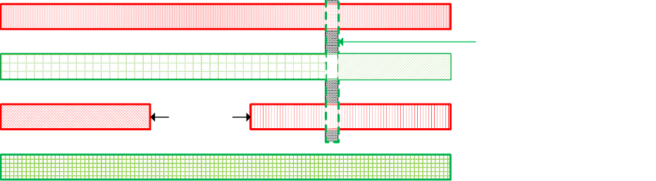
Figure 3. Cut shapes allow for the separation of continuous shapes into separate nets with less space than by same-color minimum rule. Shading patterns indicate different electrical nets.
Device Matching
Device-to-device matching is always a critical consideration in analog designs and some memory sense amp and support circuit designs. This is also true for all the latest finFET technologies, as these types of circuits are routinely integrated on the same chip as “core logic” devices and blocks. Classic techniques remain important, such as distributed common-centroid layout and center tapping of “long-tail” or differential pairs.
Such techniques, however, are eclipsed in finFET layout by the requirements for uniformity across the block layout. Design manuals provided by fabs spell out best practices for analog matching, which in most cases involve extensive use of environmental dummy devices, continuous diffusion, and constant poly density across the matching structure. Some fabs also specify the need to build matching devices on a specific fin pitch, as fins are built in groups that tend to match one another.
Electromigration and Ohmic Drops
The main purpose of the industry’s transition from planar complementary metal-oxide-semiconductors (CMOS) to finFET was to get more devices into a given area. This shift has a profound impact on undesirable mechanisms like electromigration and IR or ohmic drops. The increased transistor density leads directly to increased power density. That means more current flowing through the very thin, tightly pitched conductors and contacts low in the stack near the devices. It also allows for more current in the devices themselves.
For these reasons, it is crucial to consider these effects prior to starting layout and to have a plan for analyzing and mitigating them once the layout is complete. In some cases, preliminary analyses performed in the planning phase result in a limit on the number of fins used for a single device. Performance circuits don’t often have more than a few fins — four is a common number — due to the current draw and resulting local IR drop.
Row-based layouts will often be configured to share a supply bus between rows, a characteristic you must account for when anticipating IR drop and electromigration in the metal.
Another critical consideration is self-heating in the devices themselves and the effects of accelerating electromigration reliability failures in the metals immediately above the devices. This consideration is especially critical in finFETs based on silicon-on-insulator (SOI) technology, as the thermal conductivity of the SOI layer is typically 100 times less than that of bulk silicon.
Passive Components
All ICs have analog, I/O, or other “special” blocks in them, and finFET technologies offer a limited set of components required by these blocks. Of particular note are the film resistors. Some technologies offer base layer resistors that preclude the placement of CMOS devices in the same area. Others offer middle-of-line resistors that allow CMOS components underneath to obstruct signal and power routing on metal levels high in the stack — a significant disadvantage designers must account for when floor planning and devising the power delivery scheme.
Finger caps stacked on metal oxide semiconductor (MOS) caps are typically offered as parameterized cells (PCell) in the process design kit (PDK). These capacitors have decent capacitance per unit area. Thinned-dielectric caps are also available but at the cost of additional process steps. Inductors and T-coils are typically provided as PCells by the fab or third-party suppliers.
Very high-speed data converters that employ charge redistribution digital-to-analog converters can require very small unit capacitors on the order of 1 picofarad. Some fab and third–party IP shops provide such structures as PCells. In other cases, these elements can be manually designed, and the parasitic extraction tool can be used to confirm the capacitance.
Additionally, a PDK provides typical PNP BJTs for bandgap reference cells and temperature sensors.
The Importance of Design Tools
By necessity, IC layout and checking tools have evolved in parallel with technology. Today’s tools are no less complex than the technologies they support. While every designer has their own style and preferences for using layout tools, all layout designers must keep current with the latest offerings from design tool vendors and be familiar with the tools and techniques that can maximize productivity.
After dozens of person-years of finFET layout, here are some of the tools we feel are the most important to have in the toolbox.

1. Interactive DRC Checking Due to Lengthy DRC Runs
Design rules are exceedingly complex and number in the thousands for a modern finFET process. For that reason, design rule checking (DRC) runs can be long and produce many thousands of errors for even the smallest cell design. An iterative approach to fixing a few violations, perhaps creating others, then rerunning the full DRC can be extremely time-consuming.
A resource — like RealTime Calibre from Siemens/Mentor or Cadence’s built-in design rule notify/enforce tool — is crucial for reducing the total time to a clean DRC run. A computer-aided design team must enable these tools and work closely with the fabricator PDK.
2. Connectivity-Driven Layout
Connectivity-driven layout tools can extract and compare the connectivity of the layout to the schematic in real time. These tools are essential. In fact, the most advanced finFET technologies require the level of Cadence Virtuoso that supports this feature. Layout designers can reduce the time to a layout-versus-schematic (LVS) clean layout by working closely with the circuit designer to optimize the schematic hierarchy. The goal is to ensure both the schematic and layout stay compliant with connectivity-driven layout rules.
Two extremely effective methods of achieving a clean LVS un in one or two passes include:
- Generating device and block instances directly from the schematic
- Monitor shorts and opens in real time, often via an annotation browser sub-window
3. Width/Space Patterns (WSP) and Their Uses
FinFET process technology places severe constraints on signal and power routing, especially at the lower levels of metal. This is particularly true for standard cells provided by the fabricator or a third party, where the power supply tracks are typically pre-defined and fixed. As a result, only a few specific solutions for signal and additional power routing exist for a given metal layer.
These solutions can be encoded in a width-space pattern (WSP) in the layout design tool and stored with the layout or in a separate WSP repository. The WSPs contain valid track and color information for each layer. When creating wire routes, the wire drawing tool “snaps” the wires and vias to the predefined tracks. This is another way to achieve DRC clean layouts faster, and pre-defined WSPs are an easy way for a design team to develop and share DRC-correct track patterns for given layout block families.
4. Dynamic Selection for Hierarchy Probing
Most IC designs and layouts are hierarchically created with lower-level cells instantiated in higher levels. The tendency to do this increases as technology allows more function in a given area. Another feature that can speed up layout completion is the ability to quickly pinpoint the hierarchy level in which a specific shape resides.
Virtuoso from Cadence provides such a feature, called “Dynamic Highlighting.” We find this tool to be extremely useful in the latest finFET technology nodes due to the complexity of the design hierarchy.
What’s Next?
FinFET mask layout as we know it and practice it today is quickly yielding to the next major technology breakthrough. The next generation of technologies will be known as “gate all around,” in which the gate material completely surrounds the source and drain.
Taiwan Semiconductor Manufacturing Company (TSMC) has announced that its first implementation of a gate all around will be introduced at the 2 nm node. It will take the form of silicon nanosheets — stacks of silicon source/drain sheets with a gate material wrapped completely around them.
This is a clear continuation of the literal “upward trend” in device design. The trend is expected to drive the next innovations, including “stacked CMOS,” in which the p-channel MOS and n-channel MOS stack vertically on top of one another rather than side-by-side. At a similar time, we expect backside power/ground connected to the devices by through-silicon vias to become mainstream.
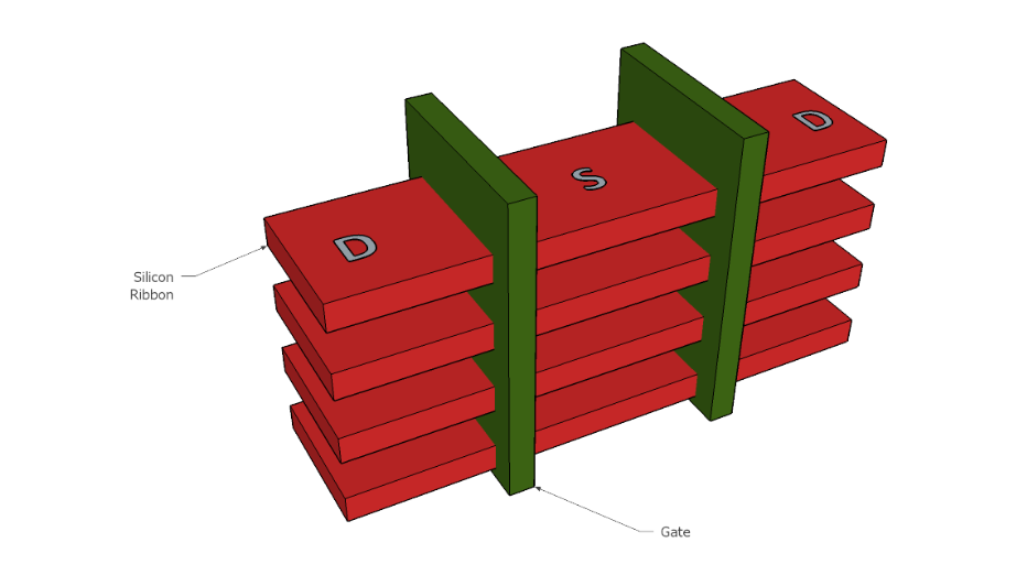
Figure 4. Nanoribbon FETs. “Fins” become stacked silicon ribbons or “sheets” surrounded by gate material on all sides.
Experience Is Key to First-Time, On-Time Layout
At ASIC North, our team of experienced layout design engineers has been working with finFET technology since 2014. We’ve delivered proven designs in Globalfoundries 14LP, IBM/Samsung FX14, TSMC N7, TSMC N5, and TSMC N3. We expect to be working in TSMC N2 by the beginning of 2024.
We have developed best practices centered around the topics discussed in this article. We look forward to bringing those best practices and our deep experience with these latest technologies to your next cutting-edge project design.
Advanced FinFET Layout Design With ASIC North
FinFET mask layouts can get incredibly complex and demand the expertise of knowledgeable designers. ASIC North understands the nuances of finFET technologies and uses industry-leading resources and techniques to offer exceptional quality without sacrificing fast turnaround times.
We’ll learn about the demands of your project and solve complex finFET design requirements either independently or as an extension of your team. Reach out today to get started or learn more about our capabilities.
Trademark Disclaimer
All trademarks, logos, and brand names are the property of their respective owners. All company, product, and service names used in this article are for identification purposes only. Use of these names, trademarks, and brands does not imply endorsement.