Today’s mixed-signal ASICs and mixed-mode IC designs can be large, task-intensive Systems on Chip that can involve complicated boundary timing. Managing these SoC risk items takes a special skill set to ensure that you have the highest chance of first pass silicon functionality. Not only does ASIC North provide world class analog and mixed signal circuit design service, we also offer top quality analog mixed signal verification (AMS) services to provide you our customers with a significantly increased level of confidence in your their fabricated product.
ASIC North will carry your IC system from start to finish in an AMS based, top-down design flow. We can significantly reduce the overall program risk with an evolving, Verilog-A based, system level schematic at the beginning of a project instead of assigning AMS verification simulations as a back-end process that can be full of surprises with little time to react. ASIC North is in the business of delivering high-quality mixed-signal solutions, not mixed-signal surprises.
ASIC North’s Approach for Mixed-Signal SoC Design AMS Design Expertise
In the field of AMS (analog mixed signal) design, there are two ways to approach a system level solution: Bottom up design and top down design.
Bottom-up Design
Bottom-up design engages a full team quickly and rapid progress can be made on all of the building blocks. The issues comes when you try to start integrating upwards. The implementation becomes less controlled and more experimental when you try to start interfacing blocks to meet system level expectations. This type of design, while technically feasible, can come with an unnecessarily arduous design cycle. Back end verification of overall system performance often requires design iterations of lower level blocks that had been considered completed earlier in the design cycle.
Why Does ASIC North Use a Top-down Design Approach for Mixed-signal SoC’s?
Our position is to work smarter, not harder. A top-down design approach gives us the ability to architect the system in a modeling environment to ensure we cover all of the specified system level functionality and I/O’s based on a set of well-defined requirements. One may ask “What if the system requirements are not well defined and the system requirements change during the design phase?” Great question!
ASIC North can work with you along the way to help understand the system as it changes and then evolve the IC solution along with it, still working to keep the design in a top down methodology. Our analog and digital design engineers work closely together to identify full system functionality requirements, performance and timing sensitive paths, multiple clock domain boundaries, start up and power down dependencies, mode switching, status/fault reporting, and signal level interfacing to name just a few.
The design phase will start with a top level partitioning, identifying which circuits will be developed by the analog design team and which functionality will be developed by the digital design team. Moving forward, an analog partitioning will occur and those analog sub-partitions will be supported by custom VerilogA models and/or additional sub-partitions. The analog portion will continue to be sub-partitioned downwards to the basic analog structures and VerilogA models will either be custom developed for all of the circuit blocks or drawn from our extensive VerilogA library. The end result will be a simulation capable VerilogA based analog system. The digital design will be partitioned in a similar fashion until all of the underlying code is either structural Verilog or synthesizable RTL.
While the development phase is in process, VerilogA models can be replaced with circuit schematics to ensure they perform as expected from a system level standpoint. ASIC North can simulate any mix of schematic and VerilogA models in a design to guarantee there are no unplanned analog system level interactions, all while reducing the time it takes to verify the analog portion of the SoC.
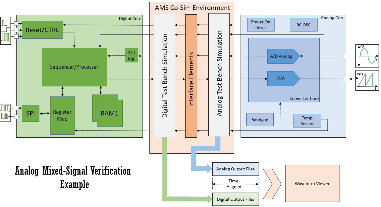
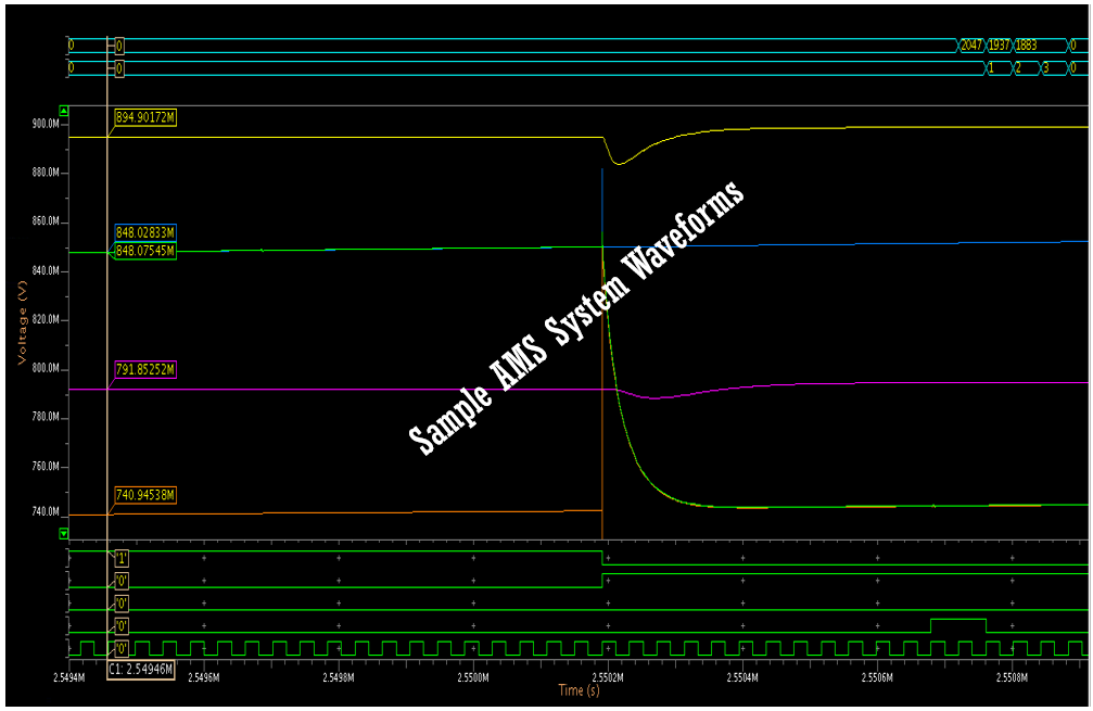
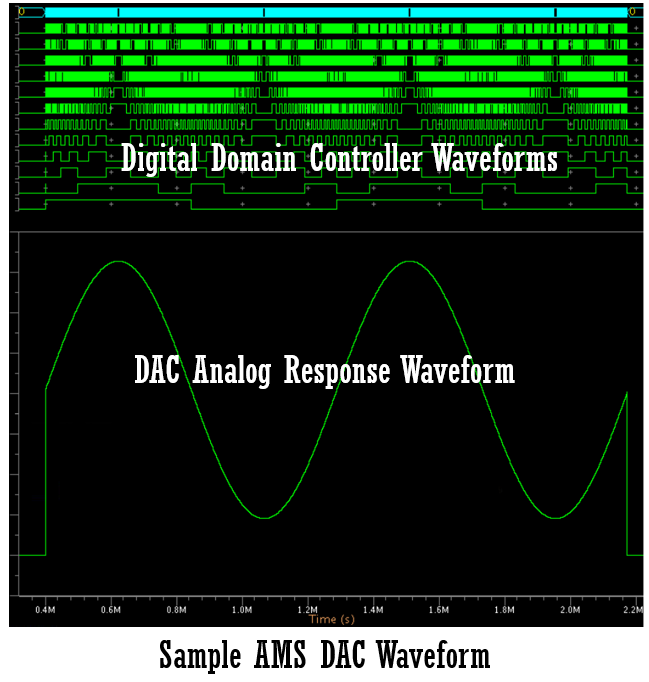
When both the digital and analog designs are integrated and ready for AMS co-sim this is where the magic happens which propels system level confidence to the next level. ASIC North’s co-sim methodology uses industry standard co-sim tool suites from either Cadence or Mentor Graphics.
Our expert AMS verification engineers use digital verification driven tests as the main engine to verify the mixed-signal functionality of the full AMS system. This results in a minimization of two independent verification paths and allows for a common verification methodology in both the digital verification and the AMS verification. A full suite of co-sim analyses that had been defined at the beginning of the program is now tracked for functionality based on a simulation schedule. Any required modifications are reported and bug-tracked until the design passes all AMS verification tests.
For customers that have critical timing paths which traverse both the digital and analog boundaries, special AMS simulations can be performed with a back annotated SDF digital view and extracted analog portions that are path relevant to confirm that the design will perform as needed. Receive Your Free Development Quote
TESTIMONIALS
See What Our Clients Say
At ASIC North, we’re here to support your mixed-signal design and verification needs with quality you can trust in the industry.
In all the years I’ve worked with Suppliers and there have been many during my 36 years at IBM…there is not a single Supplier I would rate higher than you and the ASIC North Team. The professionalism demonstrated and the dedication of the ASIC North Team is a clear reflection of what ASIC North brings to the table.
Global Commodity Manager fromIBM
“ASIC North performed excellent work for my program in helping to develop requirements for design, fab, test and delivery of a mixed-signal ASIC. They are a professional organization with significant capability. Clearly, they had our success in mind and I was happy to have them as members of my team”
Brad C., Program Manager froma Major Defense Technology Company
Contact ASIC North for AMS Design Verification Services
With all of the analog mixed-signal design companies, why choose ASIC North to develop your next SoC?
Let’s face it, developing a mixed-signal analog or mixed-signal RF SoC solution is no easy task. The key to a successful project is successful experience and ASIC North is skilled at developing mixed-signal analog and RF solutions using either a “Big A, little D” or “Little A, Big D” methodology, whichever makes the most sense for your what the customer needs.
Whether it’s a full-blown custom SoC or an analog to digital converter IC, worry less when the silicon comes back from fabrication by choosing ASIC North as your go-to design house for your analog and RF mixed-signal design needs. Contact us for a free development quote today.
 When both the digital and analog designs are integrated and ready for AMS co-sim this is where the magic happens which propels system level confidence to the next level. ASIC North’s co-sim methodology uses industry standard co-sim tool suites from either Cadence or Mentor Graphics.