Our Case Studies

ASIC North is a provider of turnkey chip design services and has a history of providing our customers a best in class experience. We work with our customers to define and then refine system on a chip (SoC) requirements that provide a solution to their product needs. Below you will find two case studies that outline how we have provided expert SoC design services to facilitate the success of our customer’s programs.

Sensor Chip

High Voltage Interface Controller

In both cases ASIC North handled the full development of the device while maintaining full transparency to our customers. From concept to delivered units we are onboard to ensure the customer experience is fully satisfying.

Case Study: Digital Modeling, Analog Modeling, & Detailed Design Flow Chart

Sensor Chip

This effort supported a customer in the development of a sensor interface chip to facilitate their product development into a new market. ASIC North was selected from a field of 12 design houses to service their turnkey mixed-signal ASIC development.

Specification development

During the specification development phase ASIC North worked with the initial requirements and architected a solution that met requirements and could be reliably manufactured while meeting aggressive cost targets. The feature set for this design was as follows:

  • An internal RC-Oscillator trimmed to +/- 8% accuracy
  • Multiple 12b ADC’s and DAC’s connected to an array of sensor channels
  • Custom digital sequence controller which provided Signal processing of the stored samples and prepared them for Burst transfer to the centralized processing device
  • SPI interface for off-loading processed data and configuring the device
  • A 64-bit eFuse block to hold calibration values
  • Two voltage regulators to maintain constant internal supply voltages with a changing battery voltage

The output of this phase was a mutually agreed upon engineering specification that the design team could use for each of the constituent blocks within the design. The semiconductor fabricator (FAB) and technology process were also selected during this phase as part of the requirements.

Learn More

Closeup view of the inside design of a microchip

Design Execution

Design Enablement

To ensure first time success, a design flow was selected that provided a comprehensive verification strategy. This verification included block level spice level simulations at twelve (12) process corners, digital verification of Register Transfer Logic (RTL) and synthesized gate level netlists and Analog Mixed Signal (AMS) verification of the entire design.

Next a methodology document for the project was defined to provide clear guidance as to how the design activities would proceed. This document outlines the required simulation tools and conditions as well as layout assumptions which guarantee physical block integration will proceed smoothly. There are many right ways to handle VLSI design however, for expediency, we needed to be sure that all designers were following the same process. This document guided the team to provide consistent deliverables that could easily be integrated into the chip.

Reviews

There were three major levels of review that occurred during the development. These checkpoints included the customers’ team to allow a collaborative decision process about any course corrections that needed to be made for the program.

  1. The first review was the schematic level review and included block as well as chip level status.
  2. The second review was a layout level review and included simulations that accounted for parasitic contributions from the completed layout.
  3. The final review was conducted just prior to release to manufacturing. All action items which were identified and tracked to closure through regular collaborative meetings with the customer were reviewed and the design was released to the Fab

Characterization

Production Ramp time and low unit costs were a priority for this project. Consequently, we selected a supplier with a strong connection to our outsourced assembly and test (OSAT) partner and who had the same test equipment which would be used for production testing in Shanghai. Our team worked side by side with this supplier to develop the characterization and production test programs and interface hardware. Although the characterization test bring up took approximately 25% longer than initially scheduled, the production ramp proceeded ahead of schedule with a net result of an on time delivery of production parts for our customers’ end of year targets.

Qualification

Qualification proceeded according to JEDEC JESD47 “Stress-Test-Driven Qualification of Integrated Circuits” which outlines standards for both semiconductor devices and packaging. Hardware was selected for multiple production lots as specified by JEDEC. There were no anomalies noted during the qualification. ASIC North provided a complete Qualification report to the customer as required by our contract.

Manufacturing

The manufacturing phase included working with the Fab to approve and create the masks, schedule engineering and production hardware, and work with our OSAT partner to handle the assembly, test, qualification and production of the product. For this program ASIC North managed the supply chain for all aspects of the manufacturing process.

Once the design was fully qualified, ASIC North delivered 4.7 Million units to our customer on the schedule identified within the original contract. Fabrication and Assembly yields averaged above 98% with no known design limited yield detractors.

High Voltage Interface Controller

This effort supported a Military-Aerospace company in the development of a custom ASIC for their system. This was a flip chip design that needed to be managed as an International Traffic in Arms Regulations (ITAR) program. ASIC North was responsible for developing the engineering specification, design, fabrication, bumping, test and characterization of the device.

Specification development

During this phase, ASIC North took the initial requirements and collaboratively worked with the customer to architect a solution that could be manufactured in a high voltage technology. The feature set for this design was as follows:

  • 4 power domains (+10v to -22v)
  • 12b Digital to Analog Converter (DAC)
  • High Voltage Driver fault condition handling
  • High current/High voltage drivers
  • Customized digital controller
  • SPI control interface

The output of this phase was a mutually agreed upon engineering specification that the design teams could use as their design source details for each of the blocks within the design. A compliance matrix was developed to capture status and compare to specifications through all phases of design and test.

Learn More

VLSI Design image

Design Execution

Design Enablement

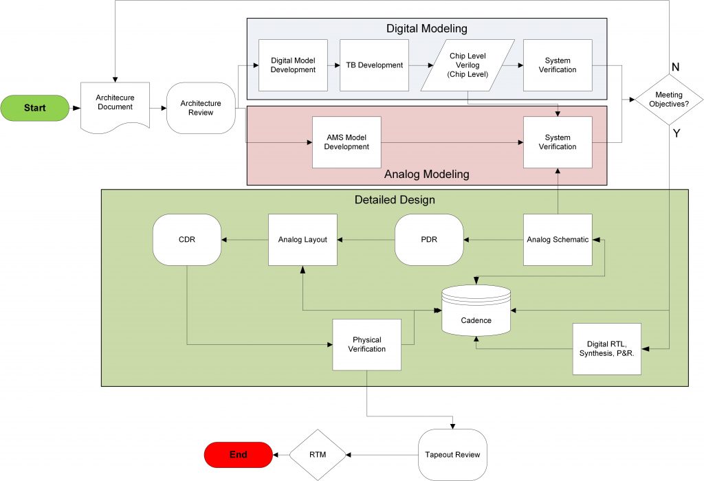
The choice for the design flow was selected to enable a comprehensive verification strategy being in place to ensure first time success. This validation included block level spice simulations, digital verification and AMS verification.

As in the 1st case study, a methodology document for the project was defined to provide clear guidance to the team as to how the design activities would proceed. As stated earlier, this document guides the team to provide consistent deliverables that could easily be integrated into the chip.

Reviews

There were four major levels of review that occurred during this development. These checkpoints included the customers’ team to allow a collaborative decision process to provide for course corrections that needed to be made for the program. At each review the compliance matrix was reviewed and updated to demonstrate how the design performance compared to specification requirements.

  1. The first review was the architectural review. This phase essentially reviewed the engineering specification to ensure that the assumptions made for the device would result in a design that met the overall requirements.
  2. A schematic level review included block level simulation results which proved the feasibility of meeting performance targets. Design and verification methodologies were reviewed to demonstrate the device would be thoroughly checked to insure proper operation under all manufacturing and environmental conditions. Finally, a preliminary review of the device floorplan demonstrated it would meet the customers’ size and signal interface constraints.
  3. The third review was a layout level review and included simulations that accounted for parasitic contributions from the completed layout.
  4. The fourth review was for database release to manufacturing.

Actions for all reviews were identified and tracked to closure through regular collaborative meetings with our customer.

Characterization

As noted previously, this project was subject to ITAR rules which dictated that fabrication, characterization, qualification and production testing be conducted domestically. ASIC North subcontracted this work to a US based facility specializing in lower volume testing for US Military and Aerospace projects. ASIC North Engineers developed the necessary test patterns for device configuration which were then converted to test programs for the selected characterization and production test platform.

All Engineering hardware provided to our customer worked flawlessly in their system test environment. However, characterization testing was delayed due to devices being damaged by incorrect power supply initialization on the characterization tester. ASIC North Engineers traveled to the suppliers’ facility to work alongside of the suppliers’ test engineers during the debug efforts. Our engineers were able to diagnose the problem and demonstrate the failure mechanism in simulation. This resulted in a modified power supply sequencing plan on the tester. Subsequent testing proceeded without incident and a full characterization report was provided to the customer.

Qualification

For this project, Qualification of the device is being completed by the customer as part of their system qualification. No unique device qualification was required.

Manufacturing

As noted above, the manufacturing phase included working with the Fab to approve and create the masks, schedule engineering and production hardware, and work with outsourced assembly and test (OSAT) partners to handle the assembly, test, qualification and production of the product. For this program ASIC North managed the supply chain for all aspects of the manufacturing process.

ASIC North is in the process of currently delivering production units for this development.