Jump to:
Wireless Communications have become an integral part of everyday life, from broadcasting, networking, toys and inventory control to the medical field. Radio frequency (RF) circuits support a wide range of applications. RF integrated circuits (RFICs) allow easy access to the radio spectrum in myriad ways. They enable users to combine their unique characteristics with other electronic systems for greater flexibility, reliability, and portability.
Due to their inherently small size, RFICs allow for a higher degree of miniaturization, as in the case of battery-powered products. Unsurprisingly, the RFIC design process can vary widely and requires some specialized tools, but getting it right is critical to creating a high-performance system. Semiconductor options for integration can vary from bipolar, CMOS, and Bi-CMOS to the more exotic Silicon-on-Insulator (SOI), Indium Phosphide (InP), or other III-V technologies. Each has cost and performance advantages for differing applications.
Learn more about RFIC design and applications.
What Are RF Integrated Circuits?
Today, the RF spectrum covers a wide range of frequencies and is an extremely crowded and somewhat hostile environment. In an ever-changing and evolving environment, as new systems are developed and old ones become obsolete, frequencies are reassigned to make space for new applications or increased data rates and connectivity. The efficient use of the available spectrum is tightly regulated and controlled by government organizations such as the Federal Communications Commission (FCC).
Different frequencies are suited to different applications, so the RF spectrum is divided into sub-bands. Some bands, such as those designated for Industrial, Scientific, and Medical (ISM) applications, are open to all users, while other chunks of the spectrum are owned and operated by corporations. Worldwide, not all sub-bands are consistent for the same application. For example, the Digitally Enhanced Cordless Telephone (DECT) standard has the following allotted operating frequencies and limitations in different parts of the world:
| Country/Region | Frequency Band (MHz) | Channels |
| Europe, South Africa, much of Asia, Hong Kong, Australia, and New Zealand | 1880-1900 | 10 |
| Korea | 1786-1792 | 3 |
| Taiwan | 1880-1895 | 8 |
| Japan (J-DECT) | 1893-1906 | 5 |
| Brazil | 1910-1920 | 5 |
| Much of Latin America (excluding Brazil) | 1910-1930 | 10 |
| USA & Canada | 1920-1930 | 5 |
Worldwide DECT frequency allocation
Put simply, a DECT system designed for the U.S. market could not be exported for sale to Japan.
At the highest level of abstraction, a complete communications system is described by the 7 layers of the Open System Interconnect Model (OSI). RFICs are layer-1, the PHY or Physical layer. International specifications define and regulate operation at the PHY layer. They ensure interoperability (type approval) between Original Equipment Manufacturers (OEMs) whilst minimizing disturbance and interference to users and equipment in other parts of the RF spectrum.
With the proliferation of smart devices and the complexity of connectivity thanks to the Internet of Things (IoT), RFICs are becoming more prevalent in today’s electronics. Integration facilitates a higher component count on a single die, allowing for easier interface with other systems. Multi-chip Module (MCM) technology provides for an even higher degree of integration and miniaturization of overall functionality while leveraging the cost-effectiveness of assorted technologies for different functions, optimizing performance, and feature sets.
Careful design and packaging are even more critical at the higher frequencies due to how signals propagate and interact with their environment. Packaging can vary between traditional wire-bond, flip-chip, and Wafer Level Chip-Scale Packaging (WLCSP), or the die(s) can be encapsulated on a custom-designed multi-level laminate containing multiple RF chips and/or discrete surface mount devices (SMDs).
ASIC North has experience in designing all of the above.
What Applications Use RF Circuits?
RFICs are used in various applications, from classic terrestrial radio communications to systems using satellite links. They offer a unique advantage over other traditional discrete wireless communication methods. They can handle complex modulation schemes for higher data rates, transferring information quickly and efficiently, reaching long distances even without a clear line of sight.
Some common uses for RF circuits include:
- Communications and networking: AM/FM radio, Cordless and Cellphone, Wi-Fi, ZigBee, and Bluetooth
- Remote control and sensing: Drones, garage door openers, and keyless entry systems
- Radar: Systems used to detect and track objects in weather, automatic door openers, automotive collision avoidance, and aerospace applications
- Satellite navigation: GPS, GLONASS, and Iridium
- Imaging: Magnetic resonance imaging (MRI) machines and security scanners used in airports
- Consumer electronics: Smart devices, toys, and wireless headphones
- Medical and Health: Hearing aids and patient monitoring
- Energy Harvesting: Mesh control networks
RFICs can offer exceptional performance in many different forms of wireless communication, sensing, and control applications.
Types of RF Circuits
The terminology used to describe a radio system can often be confusing. For example, digital radio is still functionally analog — the digital operation refers to how the carrier frequency is modulated. Modulation of the carrier can be achieved by varying a single property, such as amplitude (AM), frequency (FM), and phase (PM), or combining properties for improved performance with the inevitable trade-off between bandwidth efficiency and noise susceptibility.
Some modulation schemes carry no data in the signal’s amplitude and are referred to as constant envelopes. Others contain both amplitude and frequency/phase variation, requiring a much more linear channel performance. The type of modulation may be simple and transmit a single bit per transition, or more complex, where multiple bits can be transmitted with each transition. The more complex multi-bit modulation schemes have a constellation of states, making them more susceptible to errors (an incorrect bit received), affecting the system’s Bit Error Rate (BER).
The functionality of a radio system is defined in various ways. The general operation can be termed simplex, where the communications link is in one direction. Examples include Global Positioning System (GPS), a remote control toy, or a duplex, where information is both received and transmitted. Systems with combined transmit/receive capability are often referred to as transceivers.
Duplex systems are further categorized as half or full-duplex. Conventionally, separation of the transmit and receive signals is done using time — Time Division Duplex (TDD), or frequency — Frequency Division Duplex (FDD) domains. A half-duplex system, such as DECT, is TDD, where different time slots transmit and listen. Full-duplex systems are FDD and transmit and receive concurrently. In a multi-user environment, the duplex method is further complicated by the access method, which, in its simplest form, can be by time or frequency.
Other systems, such as Spread-Spectrum, require an agile transceiver with the ability to change carrier frequencies on the fly. Spread Spectrum systems can either be fast frequency hopping or use wideband Code Division Multiple Access (w-CDMA) technology.
Radio receivers are also defined in several different ways. A heterodyne receiver is one in which the received RF signal is converted to an intermediate frequency (IF) or frequencies (there can be more than one stage of IF). For high-gain applications, the gain can be distributed at different frequencies. For many applications, filter manufacturers often have a range of standardized IF filters available.
Excessive gain at a single frequency can lead to instability due to isolation issues and regenerative feedback. A heterodyne receiver can also have greater selectivity due to the additional inter-stage filtering. A low-IF system is a heterodyne receiver that converts the received signal to a very low IF, almost, but not quite, baseband, but low enough for a digital data converter to handle, avoiding the inherent issues associated with a homodyne system. Finally, a homodyne, zero-IF, or direct conversion receiver downconverts the received RF signal directly to baseband with no intermediate frequency. Zero-IF systems require extremely careful design due to potential performance-limiting issues.
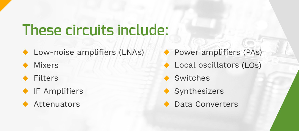
Understanding RFIC Sub-Circuits
Each RFIC contains a mixture of different sub-circuits, as shown in the block diagram. These circuits include:
![]()
- Low-noise amplifiers (LNAs): An LNA amplifies weak signals while introducing as little noise and distortion as possible. It can help establish a radio receiver’s sensitivity. Designs can be narrow band, wide band, and ultra-wide band.
- Mixers: An RF mixer combines the RF signal with a Local Oscillator (LO). Mixers can be active or passive in both the receive chain (down-conversion) and the transmit path (up-conversion). The overall objective of the mixer is to allow the receive/transmit signal to be processed at a lower frequency to minimize DC power requirements.
- Filters: RF/IF (Intermediate Frequency) filters remove unwanted frequencies, limiting signal energy to a specific frequency band. They can help prevent interference from other RF signals (blockers).
- IF Amplifiers: Amplification at frequencies generally lower than the transmit or receive frequency. IF amplifiers can be fixed or variable gain (either discrete or continuous). Variable gain amplifiers are used to control the amplitude of the signal and maintain full scale at the input of a data converter.
- Attenuators: Attenuators, active or passive, are also used to control the amplitude of a signal through a channel.
- Power amplifiers (PAs): A power amplifier boosts a low-level signal to a higher power level for transmission. The PA’s output power determines the effective range of a transmitter.
- Local oscillators (LOs): Local oscillators create the appropriate frequency for the RF signal. One of the key requirements of an LO is low phase noise (jitter) and a wide tuning range to cover the frequency bands of interest. The frequency of an LO is stabilized using a synthesizer.
- Switches: Switches connect and disconnect signal paths within an RF circuit. They can help route signals, match impedance, tune antennas, and switch between operational modes. RF switches need to have a low insertion loss when on and high isolation in the off state.
- Synthesizers: Synthesizers are used to control and stabilize the frequency of the LO. As a complete sub-system in their own right, they can contain prescalers, dividers, charge pumps, loop-filters, and phase detectors. Synthesizers can be fractional or integer-N, fractional-N.
- Data Converters: Data converters take two forms and are required to convert the received data from analog to digital format (ADC) for processing by other parts of the system or conversion of the digital data to analog (DAC) for transmission.
How Are RF Integrated Circuits Designed at ASIC North?
Designing an RFIC is highly varied. In addition to circuit simulators, an engineer may use additional tools, such as electromagnetic simulation, for interconnecting and package parasitic modeling and design. Development starts with high-level design specifications and ends with bottom-up verification to check functionality and connectivity. The general workflow for designing an RFIC is as follows:
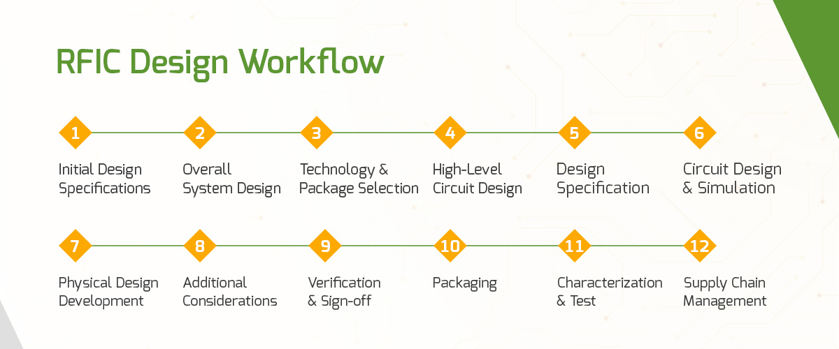
RFIC Design Flow
1. Initial Design Specifications
As mentioned earlier, the design of an RF system generally starts with an internationally recognized standard that defines the system’s operational parameters. High-level specifications are developed from this document, identifying key functions, constraints, and topologies. Certain elements that need definition are the desired operational frequency range, power output, input sensitivity, noise figure, linearity, and bandwidth.
2. Overall System Design
A high-level system design is conducted to define the system’s overall architecture and determine each sub-circuit’s top-level requirements. Applicable tasks might include block diagrams to visualize how the components connect, a trade-off analysis to balance different design options, and system performance simulations to assess and optimize a final design. Constraints, such as pin-out, isolation requirements, and DC power supply budgets, are also determined.
3. Technology and Package Selection
The selection of appropriate partners for foundry technology (bipolar, biCMOS, CMOS, and so on) and packaging is crucial to the first-pass success of any product. The choice of features, such as the number of back-end-of-line (BEOL) metal layers and mask-related component features, such as high-density MIM capacitors, affects the final cost. Additional considerations include production quantities and product/technology lifetime.
4. High-Level Circuit Design
A hardware description language (HDL) model used during preliminary circuit design allows the engineer to visualize how the system responds to signals with different levels of complexity and how a system should be partitioned. Mixed-level AHDL and circuit simulation enable the performance of very specific high-risk and/or critical parts to be analyzed.
This step aids in the specification of these components and assists in predicting performance when combining sub-circuits of the design. High-level design lays the groundwork for the final selection of the architecture to meet the required specifications and determine the performance of the sub-circuits used in the system.
In the selected technology to be fabricated, circuit design requires careful component selection from those available in the manufacturer’s (foundry) process design kit (PDK) to achieve the desired functionality. These components may include the design of spiral inductors, directional couplers, and controlled impedance lines using either planar 3D or FEM EM software.
5. Design Specification
A detailed design specification at the chip level is drafted for review with the customer. The specification includes full details of the performance of each sub-circuit, power-supply requirements, programmability, modes of operation, interface buses, and timing.
6. Circuit Design and Simulation
Circuit simulation ensures the circuit meets the required chip-level specifications across process, voltage, and temperature (PVT). Design robustness against process variation is simulated using corner models, which represent the extremes of the manufacturing process, and Monte-Carlo analysis.
Sophisticated programs, such as Cadence’s Spectre, Spice, and Keysight’s ADS, have sophisticated numerical routines to assess a circuit’s performance and behavior in both time and frequency domains. A high-level simulation plan is developed for the final sign-off of the design and reviewed with the customer to ensure that all aspects of critical channel performance are covered.
7. Physical Design Development
Layout and mask design for manufacturability is crucial as the feature size of integrated components shrinks and the cost of mask manufacture increases. Layout optimization is achieved through tasks like:
- Electromagnetic simulation and extraction
- Parasitic extraction and back annotation
- Layout vs. schematic (LVS)
- Design rules check (DRC)
- Electrical rules check (ERC)
- Analog/Mixed-Signal Simulation (AMS)
- ESD Analysis
These tools help design RF interconnects, check connectivity and functionality, and follow high-frequency electro-migration and manufacturability design requirements.
8. Additional Considerations
Before a design is submitted to a foundry, several additional issues must be considered. For example, will the design use a stand-alone mask set, or will the cost of prototype manufacture be offset by sharing the mask costs with other designs (pizza mask)? Additionally, good RFIC design practice over-engineers the base layers of the wafer to ensure spare components are available for connection at minimal cost, using a simple metal mask change should performance dictate.
9. Verification and Sign-off
Final performance and functionality of the complete system to ensure overall system specifications are met prior to tape-out to the foundry for mask manufacture and fabrication. Typically, the customer reviews a compliance matrix of all key design parameters for sign-off (acceptance of the design).
10. Packaging
RFIC packaging comes in many styles. ASIC North can help you navigate the pros and cons of different package styles based on the design particulars of your solution, whether it is a wirebond QFN or a custom over-molded, flip-chip on laminate with LGA pads. Additionally, if there are any concerns with RF interaction between the package and the IC, ASIC North can assist with an analysis using FEM-based field solver EDA tools.
11. Characterization and Test
Physical verification of manufactured silicon performance against all design parameters is important for every RFIC design. Characterization may include skewed wafer lots to account for process variation during manufacture. Verification includes ESD and other environmental tests to determine lifetime and reliability. From the characterization data, a draft production test specification is written.
12. Supply Chain Management
Supply chain management encompasses overseeing a product through the semiconductor product life cycle – development, validation, qualification, production, and end of life. It ensures that parts arrive on a timely basis. It involves scheduling wafer starts with the foundry, package assembly and testing with the OSAT, and distribution and inventory management of finished goods.
RF Design Considerations
RF integrated circuit design can be highly individualized to the application at hand. Often, a higher level of performance and functionality can be achieved with an Application Specific Integrated Circuit (ASIC) as opposed to a discrete design. Besides the initial specification, the Systems Engineer is encouraged to develop a “wish list” of performance features and enhancements for open discussion with the team at ASIC North.
The following aspects of the RF design will need consideration:
- Performance budgets: The system-level design for RFICs typically sets a “budget” for certain parameters, such as transmit power, phase noise, noise figure, linearity, harmonics, and DC Supply Voltage and Current consumption (operating power dissipation).
- Design Constraints: Depending on the frequency of operation, additional discrete components may be required to support the operation of an ASIC. Integrating all components, such as baluns and filters, may not be cost-effective due to physical size and the required silicon area.
- Simulation: Designing an RFIC typically calls for several iterations of simulations, including circuit simulation, EM, and parasitic extraction. Many external factors can affect an RF circuit’s performance, such as the location of external circuits, temperature, and electromagnetic environment. Good simulation techniques can help account for these factors and aid in the optimization of the final design.
Partner With ASIC North for RF Design Expertise

There is a lot that goes into designing RFIC solutions. If you lack experience in this area, consider hiring a professional team. At ASIC North, we have the expertise and industry contacts to take a design from concept to production. We take the time to develop integrated solutions designed to meet your unique operational needs. The ASIC North team can meet your critical RF design requirements with a wide range of technologies, including specialties in the design of critical blocks such as PAs, LNAs, and synthesizers.
ASIC North can build full-featured RFICs thanks to extensive in-house design capabilities, so you can interface with the right systems and meet all applicable specifications. Reach out today to learn more about ASIC North’s experience in the RF markets and how we can help you design a custom RFIC for your next program.