Jump to:
FinFETs form the foundation for many of today’s semiconductor fabrication techniques but also create significant design concerns that affect your layout. Understanding the changes and design strategies that finFET requires is crucial to building an effective layout. In this post, we’ll talk about how these changes influence integrated circuit layout.
The Emergence of FinFET Technology
With each generation of integrated circuit technology, custom physical layout becomes more and more challenging. From the days of manually cutting shapes into Rubylith to today’s computer-aided design, layout rules have grown exponentially in number and complexity to accommodate the ever-increasing density of the underlying transistors.
For decades, planar complementary metal oxide semiconductor (CMOS) integrated chip (IC) technology followed the dictates of Moore’s Law and Dennard scaling. When physical limits started to make these trends falter in the early 2010s, there was only one way for planar CMOS to go: up. When that happened at the sub-20 nanometer (nm) nodes, layout design rules and techniques took an enormous leap in complexity and constraints.
FinFET Transistor Basics
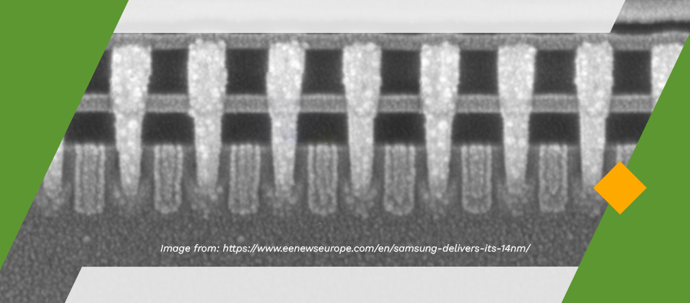
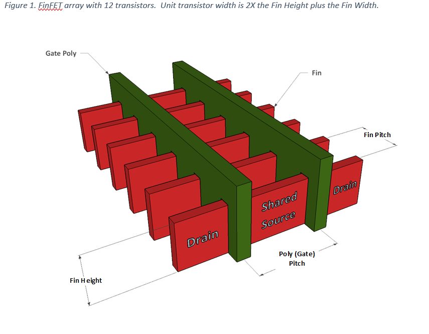
A finFET — a type of field-effect transistor (FET) — can be envisioned as a traditional planar CMOS transistor turned on its side so that the gate polysilicon can interface with the source and drain on two surfaces. The vertical structure where transistor action occurs is called a “fin” and is fabricated from doped silicon.
The fins can be constructed on bulk silicon, in which case they must be isolated in much the same way as in planar CMOS. They can also be on top of an insulating layer as in silicon-on-insulator (SOI) CMOS. The gate poly is deposited such that it runs up one side of the fin, over the top, and down the other side. The channel is formed everywhere the poly contacts the fin.
FinFET technology has a couple of implications. Most importantly, the height and width dimensions of the silicon fins are set by the fabrication process and not by the circuit designer. This means the width dimension of each transistor is set by the number of fins that the gate poly crosses rather than the width of the diffusion shape. Hence, all transistor widths are quantized as an integer number of fin crossings, each of which adds approximately 10-100 nm to the width depending on the process.
Additionally, the fins are fabricated on a regular grid, and all fins in all blocks must be aligned to this grid. This constrains the placement of transistors within a block and blocks within a layout. Further, in the most advanced technology nodes, the gate poly strips are also on a grid, resulting in placement constraints in both X and Y dimensions.
Published tear-downs of finFET devices reveal that the fin grid pitch is around 30 nm, and the poly grid pitch (also known as the contacted poly pitch) is around 50 nm.
Transistor gate poly lengths are not quantized but are severely restricted. In most finFET technologies, only two or three gate lengths are permitted: one for the minimum or “core” length, one for medium voltage analog and custom circuit applications, and one for input/output circuits.
As usual, the fabs provide special rules for memory array and support devices. These rules typically allow a higher density for array core devices while not severely impacting partial- and all-good array yields.
The grid-based nature of device placement and limited gate length selection lead to the first rule of finFET mask design: regularity and uniformity affect the device performance and hence are required by the layout design rules.
The Importance of Planning
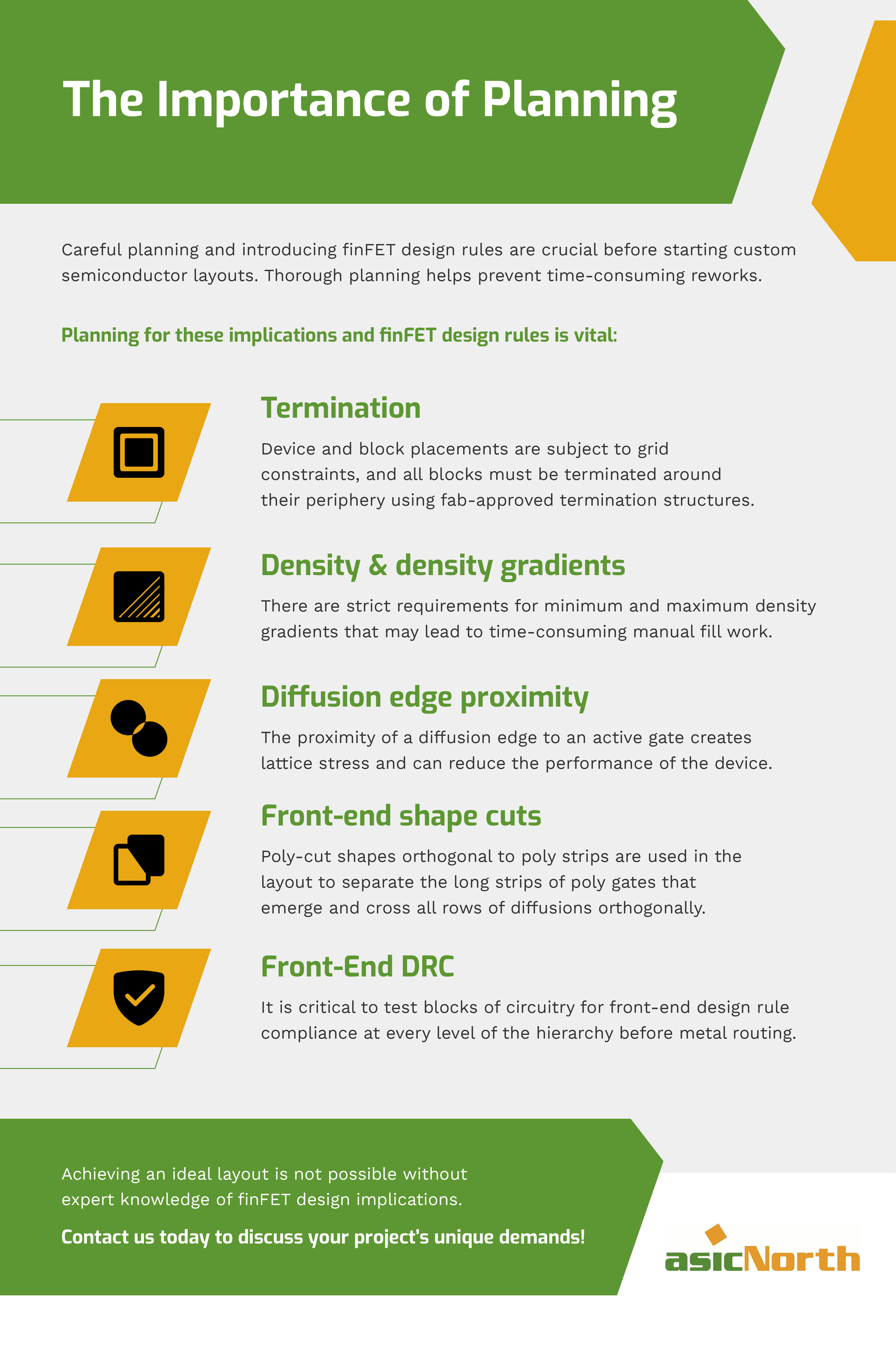
In custom semiconductor layouts, careful and thorough planning before starting the layout has always been an important practice for successful chip design. The introduction of finFET design rules makes it essential for preventing time- and area-consuming rework at critical stages of the mask design.
Termination or “Finishing”
FinFET technology design rules do not allow blocks of circuitry to be placed arbitrarily. In addition to the grid constraints for device and block placement, all blocks — from the smallest op amp to large intellectual property (IP) blocks — like phase-locked loops and data converters — must be terminated or “finished” around their periphery using fab-approved termination structures.
As always, the substrate and any N-wells must be biased. The area required for these boundary and tap structures can easily be an order of magnitude more than a small structure comprising, for example, a few logic gates or an “antenna” diode. Adding such structures late in the layout cycle as logic ECOs or when routing antennas are discovered can be very difficult and time-consuming because of the area requirements.
Density and Density Gradients
One of the many causes of layout-induced variability in today’s finFET technologies is shape density and density gradients. This is especially true for the poly gates, and hence there are stringent requirements for minimum density, maximum density, and density gradients that must be considered at floor-planning time. If the automated fill algorithms that are used to meet these density-related ground rules cannot find a valid solution, time-consuming manual fill work and possibly even relocation of large blocks might be required.
Density gradient constraints kick in when blocks built from minimum gate length devices are placed next to blocks built from the longer gate devices. Such placement may require a large transition region or special fill shapes to meet the density gradient rules.
While the poly and diffusion density rules have the greatest effect on the electrical performance of the devices, most metal layers also have minimum and maximum density limits. In most cases, the automatic fill algorithms will be able to create Design Rule Checking (DRC)-correct solutions for these rules.
It is possible, though, to create a DRC–correct layout that does not meet metal density rules and cannot be solved by the fill algorithms. This is another case where time-consuming manual effort is required to fix the density violations. To avoid this occurrence, a simulated fill algorithm should be incorporated as part of layout DRC checking at lower levels.
Diffusion Edge Proximity
With the advent of ubiquitous shallow-trench isolation in the early 2000s, the effects of crystal lattice stress on device performance became well–known. In fact, many technologies purposely introduced tension/compression stress films over devices to mitigate or even take advantage of these effects.
In finFET layout, the proximity of a diffusion edge and its shallow trench isolation to an active gate creates lattice stress that can significantly degrade the performance of that device. As a result, fabs strongly recommend a certain specific distance or number of poly pitches be observed between an active device and the edge of the diffusion area. Since any break in the diffusion will require this spacing, it’s often more efficient to observe a practice known as continuous diffusion.

In this approach, spaces between devices are filled with dummy devices in an electrically off state rather than a diffusion break. Note that changing fin counts also requires a diffusion break or dummy device, so most blocks are designed to use a consistent number of fins per device with the device width set by the number of gate fingers. These constraints result in row-based layouts with devices in a given row all having the same number of fins.
Further, to comply with termination rules, each row has the same length in the direction orthogonal to the gate poly. Dummy devices with the same number of fins are placed between functional transistors and termination structures on the end of the row. These devices must be accounted for and included in the schematic to pass LVS checking and give the circuit designer information about leakage from active diffusions to supplies.
Another well-known proximity effect, N-well edge proximity, is not generally considered a significant source of variability in finFET layout. This is likely the result of continuous diffusion practices effectively enforcing minimum spacing between N-well edges and active devices.
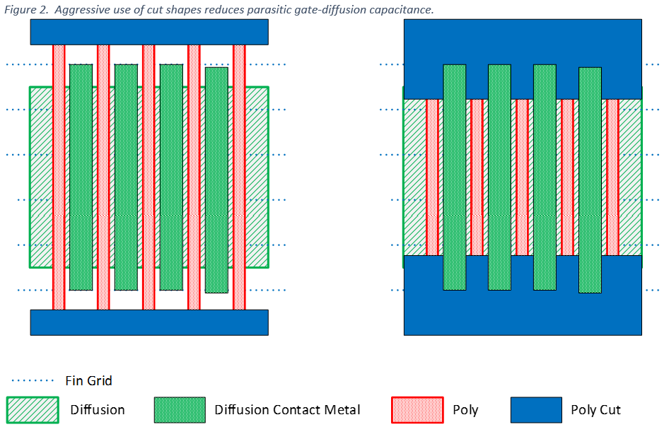
Front-End Shape Cuts
As a finFET block layout takes shape, a regular structure with rows of consistently-spaced diffusions on some multiple of the fin pitch emerges. Poly gates will be in long strips crossing all the rows of diffusions orthogonally. To separate the strips into individual transistor gates, poly–cut shapes orthogonal to the poly strips are used in the layout. These shapes allow the poly to be broken with less spacing than the required minimum spacing or termination for drawn poly shapes.
Diffusion contact breaks can be created in the same fashion. While design rules constrain the locations and sizes of the cut shapes, there can be some flexibility in their geometries that can be used to reduce parasitics or increase density if the layout designer knows how to apply it.
Front-End DRC Before Routing
It’s critical that blocks of circuitry at each and every level of the hierarchy be tested for front-end design rule compliance before any metal routing occurs. Reworking blocks to meet termination, continuous diffusion, density rules, and cut shape placement — among many other constraints — is difficult and time–consuming enough without having to worry about re-routing wires and rearranging power grid structures.
Front-end DRC compliance for very low-level cells like standard logic gates should be tested in situ in a prepared testbench layout. Then, any violations with typical adjacent cells can be seen and corrected in the IC mask design. For example, when cut shapes are placed close to the edge of a cell, they can interact with cut shapes in an adjacent cell to create a shape that’s smaller in area than the design rules permit.

FinFET IC Mask Design Services From ASIC North
For many semiconductors, custom layouts are the only way to accommodate the complexities of finFET technologies. Working with these transistors calls for expertise from knowledgeable, seasoned IC mask designers like the ones at ASIC North. We use industry-leading tools and checking strategies to deliver high-quality work in shorter timeframes.
At ASIC North, we take the time to understand the unique demands of your project and can tackle even the most complicated IC mask designs. We can work independently or partner with your team to create the ideal finFET layouts for the application. Learn more about our capabilities, or reach out to us to discuss your project!